Bridging the Gap: Why eFPGA Integration is a Managed Reality, Not a Schedule Risk

In the high-stakes world of aerospace and defense (A&D) microelectronics, the primary currency isn’t just performance—it’s predictability. When architecting a new ASIC, the specter of “unknown unknowns” is what keeps Program Managers awake at night.
A common friction point in adopting embedded FPGA (eFPGA) technology is the perceived schedule risk associated with integration overhead. Critics often point to the complexity of the ASIC flow, citing that adding reconfigurable fabric is a bridge too far for tight delivery timelines. Even the National Security Agency (NSA), in its Commercial eFPGA Evaluation Report, noted that eFPGAs “require some additional work to integrate into an ASIC compared to other commonly used hard IP.”
As a leading provider in the eFPGA IP space, we don’t run from that statement—we burn down that risk. The “additional work” is not a mystery; it is a well-defined, repeatable engineering work package. By shifting the perspective from “exploratory risk” to “structured implementation,” it becomes clear that eFPGA technology is ready for prime time in the most demanding defense schedules.
The Myth of the “Integration Black Box”
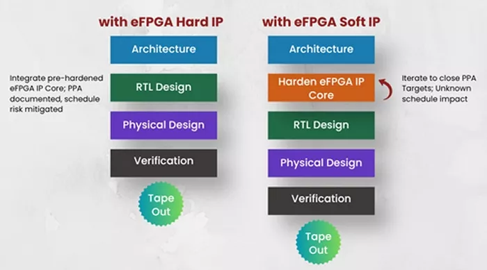
The fear of integration overhead usually stems from the era of “soft” IP cores. When a vendor delivers a soft IP fabric, they are essentially handing the Lead Architect a massive pile of RTL and saying, “Good luck with timing closure.” In that scenario, the burden of physical implementation, power grid design, and signal integrity falls entirely on the Prime contractor. That is where schedule slips happen.
Modern eFPGA IP, however, is delivered as a Hardened Macro. This distinction is the difference between being given a pile of bricks and being delivered a pre-fabricated room.
This topic is discussed in more detail in our previous blog (https://www.quicklogic.com/2026/03/24/tapeout-predictability-with-hardened-efpga-ip-blocks/)
Integration as a Known Work-Package
When we deliver eFPGA IP, we aren’t delivering a puzzle; we are delivering a completed component with a comprehensive “Integration Kit.” This kit transforms the integration process into a series of standard EDA (Electronic Design Automation) tasks. We break this down into five key pillars of predictability:
1. Complete EDA Views
We provide the same LEF, GDSII, Liberty (timing), and Verilog models that one would expect for any standard Hard IP, such as SRAM or high-speed SerDes. The ASIC team treats the eFPGA as a “black box” with known pinouts and timing constraints. There is no “filling in the gaps.”
2. Reference Integration (The Playbook)
We supply reference integration flows. These serve as a blueprint, including AXI/APB wrappers, clocking strategies, power-domain templates, and test benches. Instead of asking “How do we integrate this?”, teams follow a validated playbook.
3. Documented Roles and Responsibilities
One of the biggest sources of schedule risk is unclear ownership. Our delivery defines exactly where the IP vendor’s responsibility ends and where the SoC integrator’s begins. This clarity eliminates the “gray areas” that cause project stalls.
4. Deterministic Bitstream Loading
The “additional work” noted by the NSA often refers to the configuration logic, meaning the supplemental IP used to configure the eFPGA Hard IP. By providing standardized bitstream loading flows and configuration controllers, we turn “how do we program this?” into a standard boot sequence used in FPGA chips.
5. Clear Sign-Off Criteria
Integration risk often comes from shifting definitions of “done.” With hardened eFPGA IP, sign-off is explicit: timing closure against delivered models, power validation within known envelopes, and functional verification using provided test benches.
Countering the “Additional Work” Argument
Is there “additional work” compared to implementing a simpler IP block, such as a standard PLL? Yes. But an eFPGA is a sophisticated subsystem, not a single-function block. The work is deterministic. A deterministic task is not a risk as it has a well-understood implementation timeline.
In fact, the “work” of integrating an eFPGA is significantly less than the alternative: the “re-spin risk.” If a team developing a fixed-function ASIC discovers a bug in its DSP pipeline or needs to update a cryptographic algorithm post-tape-out, the schedule risk isn’t measured in weeks—it’s measured in years and millions of dollars for a new mask set.
By spending a few weeks on a structured eFPGA integration work package today, you are effectively buying an insurance policy against the catastrophic schedule failure of a hardware re-spin tomorrow.
Reframing the Conversation
The defense sector doesn’t require zero integration effort—it requires accountability and repeatability.
The perception of eFPGA as a schedule gamble is rooted in outdated assumptions. In reality, modern hardened eFPGA IP aligns perfectly with program needs:
- Configuration Control: Versioned IP and toolchains ensure reproducibility.
- Auditability: Delivered artifacts support stringent compliance requirements.
- Risk Management: Defined work packages reduce uncertainty in the critical path.
From Unknown Risk to Engineered Predictability
The NSA’s evaluation of eFPGA technology isn’t a warning to stay away; it’s a call for professional, structured integration. Schedule risk doesn’t come from complexity—it comes from a lack of clarity.
By delivering eFPGA as a hardened macro with industry-standard EDA views and a transparent integration roadmap, we turn a perceived hurdle into a managed milestone. eFPGA integration is no longer an “unknown unknown.” It is a known, bounded, and repeatable work package. In an environment where avoiding surprises is paramount, that level of predictability is the ultimate strategic advantage.
Explore eFPGA IP:
Related Semiconductor IP
- Radiation-Hardened eFPGA
- eFPGA Hard IP Generator
- eFPGA on GlobalFoundries GF12LP
- eFPGA IP — Flexible Reconfigurable Logic Acceleration Core
- Heterogeneous eFPGA architecture with LUTs, DSPs, and BRAMs on GlobalFoundries GF12LP
Related Blogs
- IP Integration : What is the difference between stitching and weaving?
- IP integration: Is it the real system-level design?
- IP-XACT coming back on track
- IP-XACT Usage Survey Results
Latest Blogs
- Area, Pipelining, Integration: A Comparison of SHA-2 and SHA-3 for embedded Systems.
- Why Your Next Smartphone Needs Micro-Cooling
- Teaching AI Agents to Speak Hardware
- SOCAMM: Modernizing Data Center Memory with LPDDR6/5X
- Bridging the Gap: Why eFPGA Integration is a Managed Reality, Not a Schedule Risk